Zinc oxide thin-film transistors technology introduced for radiation-hardened applications in space
INDEPENDENCE, Mo. – Intellectual Property Developers LLC in Independence, Mo., is introducing zinc oxide thin-film transistors technology for radiation-hardened applications in space.
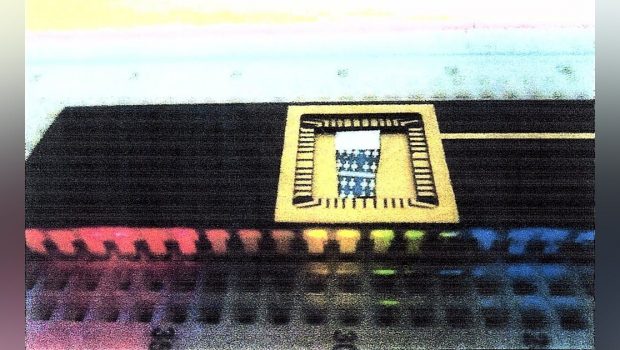
Called the ZnO Radiation-Hardened Thin-Film Transistors, the patented rad-hard space electronics technology was developed together with Auburn University in Auburn, Ala.
A thin-film transistor is made up of an annealed layer comprising crystalline zinc oxide, with a passivation layer adjacent to the thin-film transistor. The passivation layer has a thickness and material composition such that when a dose of radiation from a radiation source irradiates the thin-film transistor, a portion of the dose that includes an approximate maximum concentration of the dose is located within the annealed layer.
Related: Radiation-hardened MOSFET qualified for commercial and military satellites and space power solutions
The annealed layer has a thickness and threshold displacement energies after it has been annealed such that a difference between a transfer characteristic value of the thin-film transistor before and after the dose is less than a first threshold; and a difference between a transistor output characteristic value of the thin-film before and after the dose is less than a second threshold. The thresholds are based on a desired performance of the thin-film transistor.
The ZnO technology is radiation-hardened upon irradiation of gamma-ray radiation, and is intended for radiation hard electronics application in space, nuclear power facilities, high-altitude aviation, and other radiation environments.
ZnO technology offers reduced volume, mass, and power consumption that can operate in extreme temperature ranges.
Related: Radiation-hardened space electronics enter the multi-core era
ZnO technology compares favorably to silicon carbide (SiC), gallium nitride. ZnO technology is relatively inexpensive to synthesize device quality materials compared to GaN or SiC, Intellectual Property Developers officials say.
The company has completed a two-year research project, which shows that ZnO transistors are working well under exposure in difficult radiation situations. A patent for ZnO technology has been approved by the U.S. Patent and Trademark Office in Alexandria, Va.
For more information contact Vincent Salva, president of Intellectual Property Developers LLC, by email at vpsuss@aol.com, or by phone at 816-254-6670.


Gloss