AMD Researching Photonic Technology, Light Speed Communication On Multi-Layered Chips
AMD has shown an interest in photonic technologies and the benefits of unbelievably fast data communication for the company's semiconductors. In fact, in 2020, the company filed a patent in the U.S. Patent Office that demonstrates (on paper) a supercomputer that could allow for organically photonic-based communications systems that would link to a single chip, reports Tom's Hardware. This new advancement is another sign of just how close to the changing future we currently have reached.
AMD patent describes a future using photonics and classic technologies to achieve a hybrid future of semiconductor communications
What is photonics?
The science of photonics focuses on light waves and how to generate, detect and manipulate the source. There are two natures of light, described as wave-particle duality, having attributes of both a photon particle and a continuous electromagnetic wave. The initial goal of photonics during the 1960s was to utilize light waves to perform similar functions used by standard electronics. As we reached the fiber optic communication age in the 1980s, researchers changed the term to reflect the advancements.
Photonic technology benefits from the speed of light to allow for breakneck data communication speeds, along with the energy efficiency of using light instead of metals, such as copper, to cause a loss in the electrical currents. Having a company such as AMD researching the possibilities of combining light waves and transmitting to a single chip would permit power consumption and latency to enhance scalability and performance at a higher rate and higher level.
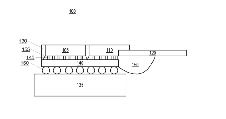
Breaking down the various levels of the above diagram, listed is:
- 100 - semiconductor chip package.
- 105 - System-on-Chip (SoC)
- 110 - photonic chip
- 120 - attached fiber optic cable
- 130 - mold compound
- 135 - single wafer substrate
- 140 - Organic Redistribution Layer (ORDL)
- 145 - microbumps attaching the SoC (105) and photonic chip (110) to the ORDL (140)
- 150 - glob top
- 155 - underfill
- 160 - standard Ball Grid Array (BGA)
The patent documentation is very technical, showing the necessary measures that AMD would take to manufacture a semiconductor chip to handle the I/O for a photonic-based component. The actual manufacturing would combine photonic and silicon-based chips placed on an ORDL.
The next step shows that the standard SoC would attach on top of the ORDL to obtain the light waves being redistributed and then carry information into and out of the specific semiconductor chip. Next, the SoC processes the data and transmits it through the ORDL to the photonic chip, which is parallel to the SoC. A fiber optic cable would carry the information transmitted from the photonic-based sector of the chip to the required destination.
AMD describes in the published designs that all of the various components can all be organized and created directly to the wafer substrate in the factory, accelerating the process for the company.
However, this cannot happen by today's current standards. Current redistribution layers are not organic, but metallic interconnects "that redistribute the I/O access to different parts of the chip," says Tom's Hardware. Such technology is similar to semiconductor leader TSMC's TSV, or Through-Silicon-Vias, which can permit two to three-dimensional chip integration.
Organic-based technologies seen currently are in OLED displays, where they use organic materials to produce light per the exposed electrical frequency.
Photonic technology could advance semiconductors to a new level, increasing scalability to achieve better energy efficiency and higher performance. The concept is highly advanced, showing that AMD is looking at new strategies to push the boundaries of what is capable by today's standards. It also taps into sciences that are not usually used in this situation.
Will we see this technology in the coming years? Probably not. The cost alone for something of this nature is not reasonable for everyday use, and would likely see AI and HPC sectors before seeing service in the home. But, it does give us hope for a future where we limit the use of dangerous and harmful materials to more organic options to sustain the environmental aspects a little longer.
News Sources: Toms Hardware , U.S Patent Office


Gloss