Union Minister Rajeev Chandrasekhar visits Gallium Nitride Technology Centre
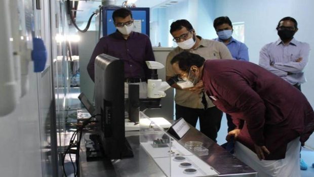
Union Minister of State for Electronics & Information Technology and Skill Development & Entrepreneurship Rajeev Chandrasekhar visited the Gallium Nitride Ecosystem Enabling Centre and Incubator (GEECI) in Bengaluru on Sunday.
Gallium Nitride (GaN) is believed to be the second most important material after silicon for electronics chips.
The facility, jointly set up by Ministry of Electronics and Information Technology and IISc Bengaluru, is aimed at establishing GaN based Development Line Foundry facility, especially for RF and power applications, including strategic applications.
"The next 2 to 3 years offer a window of opportunity for Gallium Nitride (GaN) to play a key role in enabling e-vehicles and wireless communication," Chandrasekhar said after reviewing the progress of the project and inspecting the facility.
He also saw GaN transistors fabricated in IISc Centre for Nano Science and Engineering (CeNSE) fab. The fab model in IISc will be a state-of-the-art incubation to promote indigenous development of technology, and thereby encourage final deployment into cellular infrastructure, and strategic technologies.
"Research, technology development, education and training in our institutes like IISc and IITs in the area of semiconductor manufacturing is essential to realise the dream of Digital India and fabs in the nation," Chandrasekhar said.
Creating strategic capabilities in emerging technologies is one of the core objectives of the Digital India Programme. To achieve these objectives, MeitY has drawn a 1,000 days vision that includes hi-tech/ strategic tech as an important component.
Also Read: GAIL declares second interim dividend for FY22; check details here
The minister also spoke about the Covid-induced disruptions in the global supply chains, and how the government is committed to capitalise on this narrow window of opportunity as the world is looking for a new and trusted supply chain partner.
"There is tremendous opportunity in electronics manufacturing and in the field of electronics and semiconductor design," he said.
To leverage this opportunity, the government recently announced a $10 billion incentive package for setting up semiconductor fab units in India and to also position India as a global hub for electronics systems design and manufacturing (ESDM).
Along with the semiconductor incentive package, the GaN ecosystem is also expected to drive innovation and encourage start-ups and entrepreneurs to look into business and technology seriously in the next two years. AGNIT Semiconductors Pvt Ltd, the first start-up, has already been incubated in TBI-InCeNSE, which is an incubator of SID, IISc. It has raised its first round of angel funding. It will be the first start-up to leverage the infrastructure created by GEECI.
Also Read: The Kashmir Files movie declared tax-free in Gujarat, Madhya Pradesh


Gloss